Former Google AI Researchers Secure $35M to Revolutionize Chip Design Automation
Ex-Google researchers have raised $35 million in funding to develop AI-powered tools that automate semiconductor chip design, addressing critical bottlenecks in the industry and accelerating time-to-market for next-generation processors.
Former Google AI Researchers Secure $35M to Revolutionize Chip Design Automation
A team of former Google AI researchers has successfully raised $35 million in funding to develop automated chip design technology, marking a significant investment in addressing one of the semiconductor industry's most pressing challenges: the time and complexity required to design modern processors.
The funding round reflects growing recognition that artificial intelligence and automation can fundamentally transform semiconductor design workflows. As chip architectures become increasingly complex and design cycles stretch longer, automating key aspects of the design process has emerged as a critical competitive advantage.
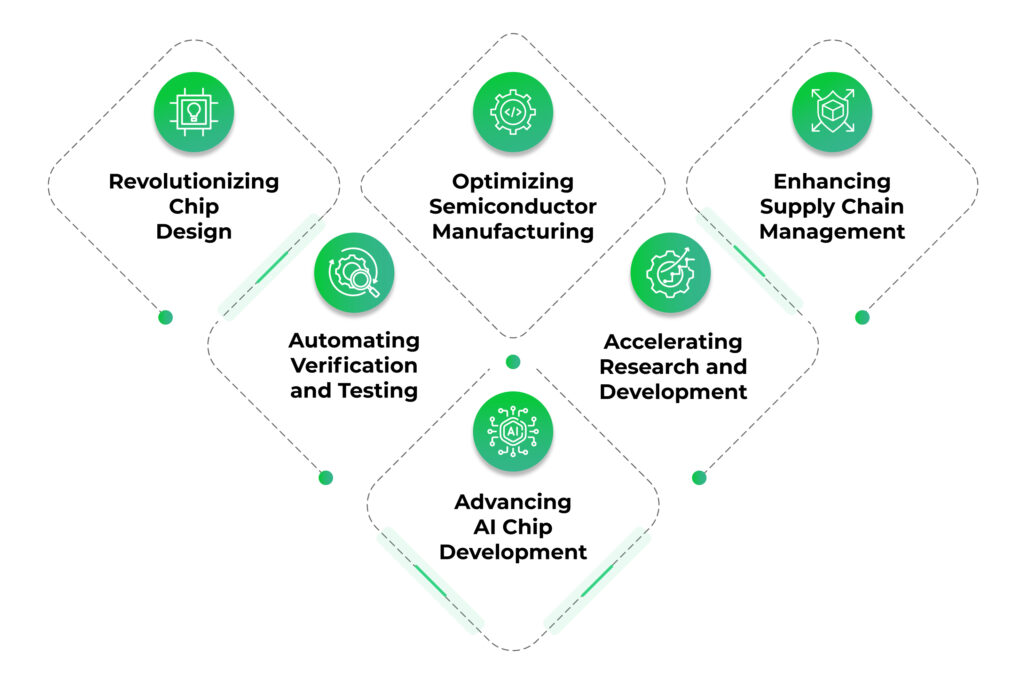
The Challenge in Modern Chip Design
Semiconductor chip design has become exponentially more complex over the past decade. Modern processors contain billions of transistors, and designing these systems requires specialized expertise, extensive simulation, and iterative refinement. Traditional design methodologies rely heavily on manual processes, expert judgment, and time-consuming verification cycles.
The bottlenecks are substantial:
- Extended timelines: Design cycles for advanced chips can take 3-5 years from conception to production
- Resource constraints: Specialized chip design talent remains scarce and expensive
- Verification complexity: Testing and validating designs requires enormous computational resources
- Market pressure: Faster time-to-market has become essential for competitive advantage
AI-Driven Automation as a Solution
The former Google researchers' approach leverages machine learning and AI techniques to automate portions of the chip design pipeline. Rather than replacing human expertise, these tools augment designers by handling repetitive tasks, optimizing layouts, and accelerating verification processes.
Key areas where automation can deliver impact include:
- Design space exploration: AI algorithms can rapidly evaluate thousands of design variations to identify optimal configurations
- Physical design optimization: Automated placement and routing of circuit components
- Verification acceleration: Machine learning models that predict design issues before expensive simulation cycles
- Constraint satisfaction: Intelligent systems that balance competing design requirements
Market Context and Industry Momentum
This funding announcement arrives amid broader industry recognition that semiconductor design is ripe for disruption. Major chip manufacturers and EDA (Electronic Design Automation) vendors have increasingly invested in AI-assisted design tools. The convergence of advanced AI capabilities, growing computational resources, and urgent industry needs has created a favorable environment for innovation in this space.
The $35 million raise positions the team to develop production-ready tools, build partnerships with semiconductor manufacturers, and scale their technology across the industry. Success in this domain could significantly reduce design cycles, lower barriers to entry for chip design, and accelerate innovation across computing, AI infrastructure, and consumer electronics.
Looking Ahead
The semiconductor industry faces mounting pressure to deliver more powerful, efficient chips at faster cadences. Automating chip design represents one of the most promising approaches to meeting these demands. By combining deep technical expertise with modern AI capabilities, the former Google researchers' venture aims to unlock new possibilities in semiconductor innovation.
As the industry continues to grapple with design complexity and time-to-market pressures, tools that intelligently automate design workflows could prove transformative—not just for the companies that develop them, but for the entire semiconductor ecosystem.
Key Sources
- Industry analysis on semiconductor design automation trends and AI integration in EDA workflows
- AWS Generative AI for Semiconductor Design and Verification documentation
- Synopsys AgentEngineer™ Technology research on AI-driven engineering workflows


